Improving infrared technology

Australian researchers have discovered a way to make infrared technology easy to use and cheap, potentially saving millions of dollars in areas using sensing devices. Their research has been published in the journal Optica.
Infrared devices are used for improved vision through fog and for night vision, and for observations not possible with visible light. High-quality detectors cost approximately $100,000, and some require cooling to -200°C.
Now, research has demonstrated a dramatic increase in the absorption efficiency of light in a layer of semiconductor that is only a few hundred atoms (0.041 μm) thick — to almost 99% light absorption from the current inefficient 7.7%. The collaborative work was conducted by The University of Sydney, UTS and ANU, including use of the NeCTAR cloud at the National Computational Infrastructure (NCI).
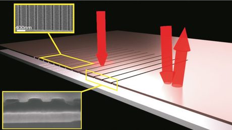
As explained by co-author Professor Martijn de Sterke from the University of Sydney, the team discovered that the ideal thin film light absorbers could be created simply by etching grooves into them.
“By etching thin grooves in the film, the light is directed sideways and almost all of it is absorbed, despite the small amount of material — the absorbing layer is less than 1/2000th the thickness of a human hair,” he said.
“Conventional absorbers add bulk and cost to the infrared detector as well as the need for continuous power to keep the temperature down. The ultrathin absorbers can reduce these drawbacks.”
Co-author Professor Lindsay Botten, director of the NCI, said the structures are much simpler to design and fabricate than using existing thin film light absorbers, which require complex nanostructures, metamaterials and exotic materials or difficult-to-create combinations of metals and non-metals.
“There are major efficiency and sensitivity gains to be obtained from making photodetectors with less material,” he said.
Furthermore, co-lead author Dr Björn Sturmberg, who carried out the research as a PhD student at the University of Sydney, said the findings did not rely on a particular material but could be applied to many naturally occurring weak absorbers.
“There are many applications that could greatly benefit from perfectly absorbing ultrathin films, ranging from defence and autonomous farming robots to medical tools and consumer electronics,” Dr Sturmberg said.
Aerosol test for airborne bird flu developed
The low-cost sensor detects the virus at levels below an infectious dose and could lead to rapid...
Superelastic alloy functions in extreme temperatures
The titanium-aluminium superelastic alloy is not only lightweight but also strong, offering the...
Water-repellent glass breaks new ground
An innovative and non-toxic process using ultrasonic sound waves can alter the surface of glass,...


